ECV
Profiler
WEP is a strong research oriented organization from the black forest area of Germany. Due to their precision engineering, they have the best technology for Electrochemical Capacitance Voltage Profiling.
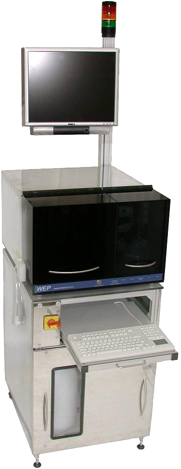

Wafer Profiler CVP 21
The Wafer Profiler CVP21 is a handy tool to measure doping profiles in semiconductor layers by Electrochemical Capacitance Voltage Profiling (ECV-Profiling, CV-Profiling) in semiconductor research or production. This ECV Profiler (CV-Profiler, C-V-Profiler) furthermore is a very good choice to analyze or develop strategies for Photo-Electrochemical Wet Etching (PEC-Etching) of semiconductors.
CVP21 supports the COMPLETE spectrum of materials:
Specification
Advantages of ECV Profiling
| Application requirement | Hall | SIMS | SRP | ECV |
|---|---|---|---|---|
| Monitor the doping concentration | ||||
| Monitor the concentration of electrically activated dopants | ||||
| Monitor the doping type (n or p) | ||||
| Monitor the crystalline quality of the sample | ||||
| Easy sample preparation | ||||
| Easy equipment preparation (no calibration or standard samples required) | ||||
| Easy contact preparation | ||||
| Substrate may be conductive | ||||
| Thickness of the epi layer may be unknown | ||||
| Depth Profile may be measured | ||||
| Depth resolution in the 1nm range possible | ||||
| Several layers may be resolved | ||||
| A broad range of semiconductors may be measured | ||||
| Concentrations below 1014 cm-3 may be measured *) | ||||
| Wafer topography may be analyzed | ||||
| Measurement without prior mechanical or lithographic preprocessing | ||||
| Photo-Electro-Chemical (PEC) etching may be evaluated | ||||
| The surface may be etched/ passivated on start of the measurement |